

Design for Test
Design for Test (DFT) is a set of techniques used in electronic design to ensure that manufactured integrated circuits (ICs) can be easily and thoroughly tested during production to identify any defects or faults. The primary objective of DFT is to facilitate the testing process, improve test coverage, and reduce the time and cost associated with testing.

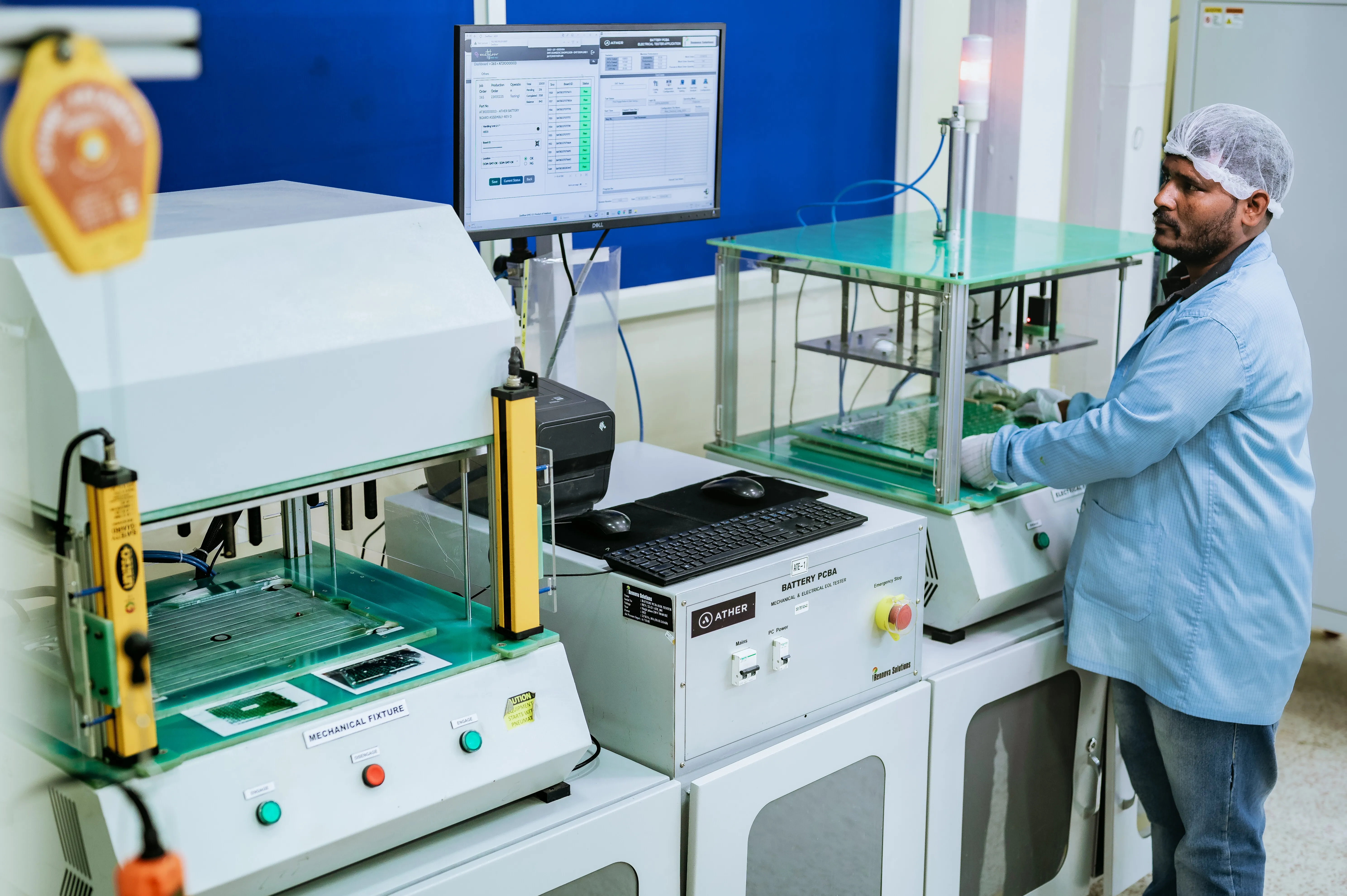
Our DFT approach begins with the integration of built-in test features directly into the design. This includes incorporating test points, access to critical nodes, and other diagnostic features that simplify the testing process.
We employ scan chain techniques to enhance testability during the manufacturing process. This involves configuring the design to allow for serial testing of flip-flops, providing efficient fault detection and diagnosis.
We incorporate boundary-scan (Joint Test Action Group - JTAG) technology into the design. This allows for efficient testing of interconnected devices on the PCB, simplifying the identification and isolation of faults.
Our DFT process includes fault simulation and design validation, ensuring that potential issues are identified and addressed before the manufacturing phase. This proactive approach minimizes the likelihood of defects and improves the overall reliability of the product.

Our history of successful projects showcases our expertise in integrating testability into the design, leading to more efficient and reliable products.
We offer comprehensive testing solutions by integrating a variety of DFT techniques. This ensures that your product undergoes thorough testing, resulting in a higher level of quality and reliability.
Our DFT services contribute to time and cost savings by streamlining the testing process. By identifying and addressing potential issues early in the design phase, we minimize the need for extensive testing during production.
We adopt a collaborative approach, involving close cooperation between design, testing, and manufacturing teams. This ensures that DFT considerations are seamlessly integrated, leading to a more efficient and reliable product.


Design for Testability (DFT) is the practice of designing products with features that make them easier to test for defects. It's important because it enhances the efficiency and effectiveness of testing processes, reduces testing costs, improves product quality, and accelerates time to market.
Designing a test involves first identifying its objectives and requirements, then selecting suitable methods and tools. It requires creating detailed test cases and procedures to cover all functionalities and failure modes, and integrating testing checkpoints into the product design for efficient access and evaluation.
We need Design for Test to ensure products can be tested efficiently and thoroughly for quality and performance, reducing testing time and costs, improving product reliability, and facilitating early detection of defects.
Design for Test (DFT) is a concept that involves designing products in a way that makes them easier to test for defects and functionality. It integrates testability features into the product design to facilitate efficient and effective testing processes.


