

PCB Layout Analysis
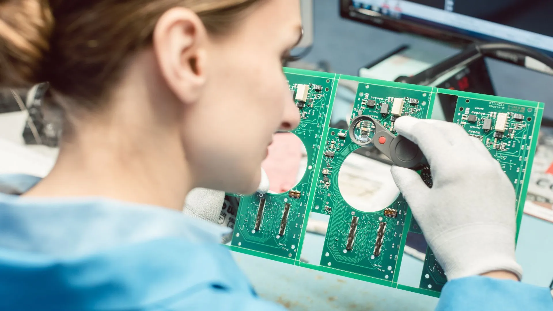
PCB layout analysis is a specialized service focused on enhancing the performance, reliability, and efficiency of electronic designs. It involves a thorough examination to ensure the PCB layout aligns with industry standards, optimizing critical aspects such as signal integrity, thermal management, and manufacturability. The analysis also aims to eliminate potential risks, such as a high rate of misplaced components or tombstones, by identifying issues related to the use of incorrect footprints or deviations from the Approved Vendor List (AVL).

Our approach begins with the utilization of cutting-edge PCB layout analysis tools. These tools enable us to dissect and evaluate every component of your design, ensuring that the layout is not only functional but also optimized for peak performance.
Our experts conduct a comprehensive analysis of signal paths, identifying and rectifying any potential issues that may compromise the integrity of your signals. This attention to detail ensures optimal functionality and reliability.
Efficient thermal management is crucial for the longevity and reliability of electronic components. Through advanced thermal simulations, we analyze the heat dissipation characteristics of your PCB layout. This proactive approach addresses thermal challenges, ensuring your design operates within safe temperature limits.
With a team of seasoned professionals, we specialize in handling intricate and complex PCB layouts. Our expertise enables us to navigate the challenges posed by complex designs, ensuring optimal performance without compromising on reliability.
Our PCB layout analysis goes beyond surface-level scrutiny. We conduct a thorough examination of every aspect of your design, from individual components to overall connectivity, ensuring a robust and reliable PCB layout.
Recognizing the uniqueness of every project, our PCB layout analysis service provides customized solutions tailored to your specific design requirements. We adapt our approach to meet the distinct challenges presented by your project.


Designing a PCB involves schematic capture, board layout, design verification using DRC and ERC, prototyping to test functionality, and adjusting the design based on prototype feedback before final production.
Planning a PCB layout includes selecting materials, determining board size, placing components strategically, routing efficiently, and considering thermal management, aligned with manufacturing constraints.
Verifying a PCB layout involves using PCB design software's DRC (Design Rule Check) and ERC (Electrical Rule Check) features to ensure the design meets manufacturing and functionality standards.
What are PCB layouts?
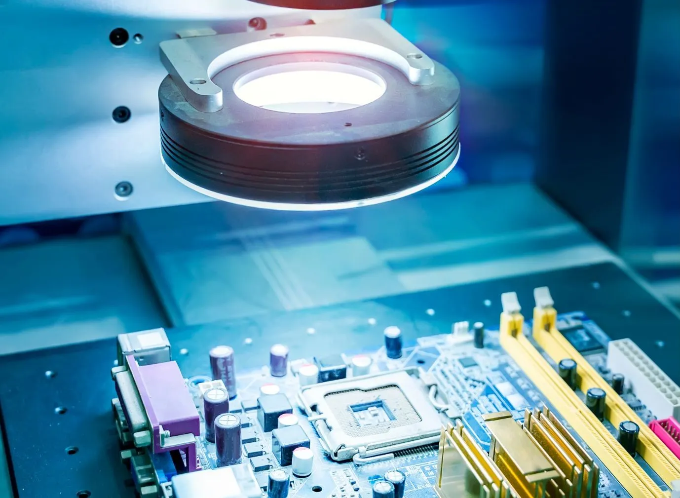
Analyzing a PCB involves using EDA software to simulate electrical functionality, signal integrity, thermal management, and mechanical stability, identifying potential issues before manufacturing.


