BGA Assembly Services
BGA Assembly Services Info
ボールグリッドアレイ(BGA)は、集積回路(IC)やその他の半導体デバイスに使用される表面実装パッケージの一種です。BGA パッケージでは、集積回路とプリント基板 (PCB) との接続は、パッケージの下側にあるソルダーボールの配列を介して行われます。これらのソルダーボールは接続点として機能し、グリッド状に配置されているため、「ボールグリッドアレイ」という名前が付けられています。

BGAのタイプ
- セラミックバッグ (CBGA):
- セラミック基板を使用しており、熱特性と機械特性に優れています。
- 航空宇宙、軍事、電気通信システムの高性能アプリケーションに最適です。
- プラスチックバッグ (PBGA):
- プラスチック基板を使用しており、費用対効果が高い。
- さまざまなサイズと構成の家庭用電化製品に適しています。
- フリップチップ BGA (CBGA):
- フリップチップボンディング技術を採用し、電気的性能を向上させます。
- マイクロプロセッサやグラフィックプロセッサなどの高速アプリケーションで一般的に使用されます。
- テープボールグリッドアレイ (TBGA):
- 組み立て時の一時的なハンダボールの配置には粘着テープを使用します。
- ハンドリングと配置の効率を高め、ソルダーボールによる損傷のリスクを軽減します。
- スタッドバッグ (SBGA):
- 電気接続用の金属スタッドまたはポストを備えています。
- 機械的安定性が向上し、自動車用電子機器や高耐久デバイスに最適です。
-
- マイクロ BGA (マイクロBGA):
- ボールピッチを小さくすることで、入出力密度を高め、デバイスを小型化しています。
- スペースが限られているモバイルデバイスやポータブル電子機器で一般的に使用されます。
Indic's BGA Assembly Services
BGAコンポーネントには特殊なはんだ付けプロセスが必要であり、当社のリフローはんだ付け技術はBGAアセンブリ特有の課題に対応するように調整されています。この方法により、はんだ接合部の信頼性が向上し、耐久性と性能が向上します。
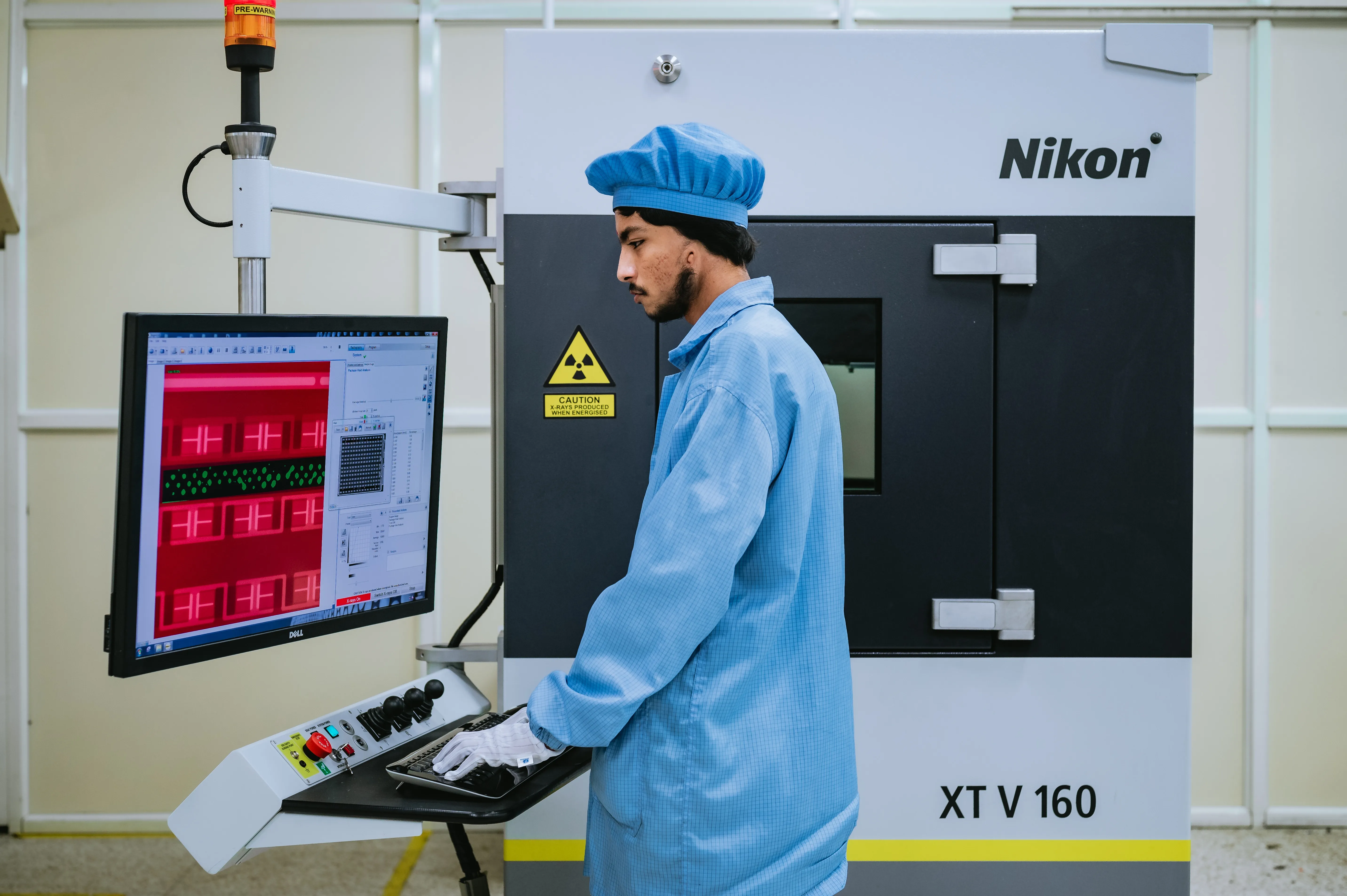
BGA品質のためのX線検査:BGAアセンブリの完全性を確保するために、X線検査技術を採用しています。これにより、BGAコンポーネントの下のはんだ接合部、潜在的な欠陥や不一致を非破壊検査で検査できます。

Flexible BGA Assembly Services
当社のBGAアセンブリサービスは多用途で柔軟性があり、さまざまなBGAコンポーネントの種類とサイズに対応します。
厳格な品質管理措置、X線検査、業界標準への準拠を組み合わせることで、最終組立製品の信頼性と性能が保証されます。


BGA Assembly Services -FAQ
A BGA package is a type of surface mount packaging for integrated circuits that uses a grid of solder balls as its connectors. These solder balls provide the electrical connections to the PCB, enabling a compact and high-density connection layout.
BGA reballing is the process of removing old solder balls from a BGA component and replacing them with new ones. This repair technique is used to fix defective BGA solder joints or to reattach a BGA component to a PCB.
BGA stands for Ball Grid Array, a type of surface mount packaging used for integrated circuits. BGA packages use solder balls arranged in a grid on the bottom of the package for electrical and mechanical connection to the PCB.
In SMT (Surface Mount Technology), BGA refers to a type of packaging used for surface-mounted devices where solder balls on the underside of the package provide the electrical connections to the PCB, allowing for high-density connections.
BGA is important in PCB assembly for enabling high-density connections, reducing PCB size, and enhancing electrical performance. Its solder ball array allows for efficient manufacturing and reliable electrical connections, critical for modern, high-performance electronics.
There are several types of BGA, including PBGA (Plastic Ball Grid Array), CBGA (Ceramic Ball Grid Array), TBGA (Tape Ball Grid Array), and MBGA (Micro Ball Grid Array), each differing in materials and specific applications.
BGA is used in PCBs to achieve higher density connections, allowing more pins in less space compared to traditional packaging. This is crucial for modern electronic devices that require compact size with high functionality.
BGA is used for its ability to provide a large number of interconnections in a small space, improving performance and reducing size. The solder balls offer better joint reliability and heat conduction, suitable for high-performance and compact electronic devices.
The process of BGA production includes creating the BGA package with solder balls arranged in a grid pattern, placing the BGA on the PCB with precise alignment, and then soldering it using reflow soldering technique to create a solid mechanical and electrical bond.
A BGA chipset refers to a chipset packaged in a Ball Grid Array format. It is used in various electronic devices, such as computers and smartphones, for its efficient space utilization and reliable connections.
BGA assembly is the process of attaching Ball Grid Array (BGA) components to a printed circuit board (PCB) using surface mount technology (SMT) techniques. It involves applying solder paste, placing BGA components, and using reflow soldering to establish the connections.