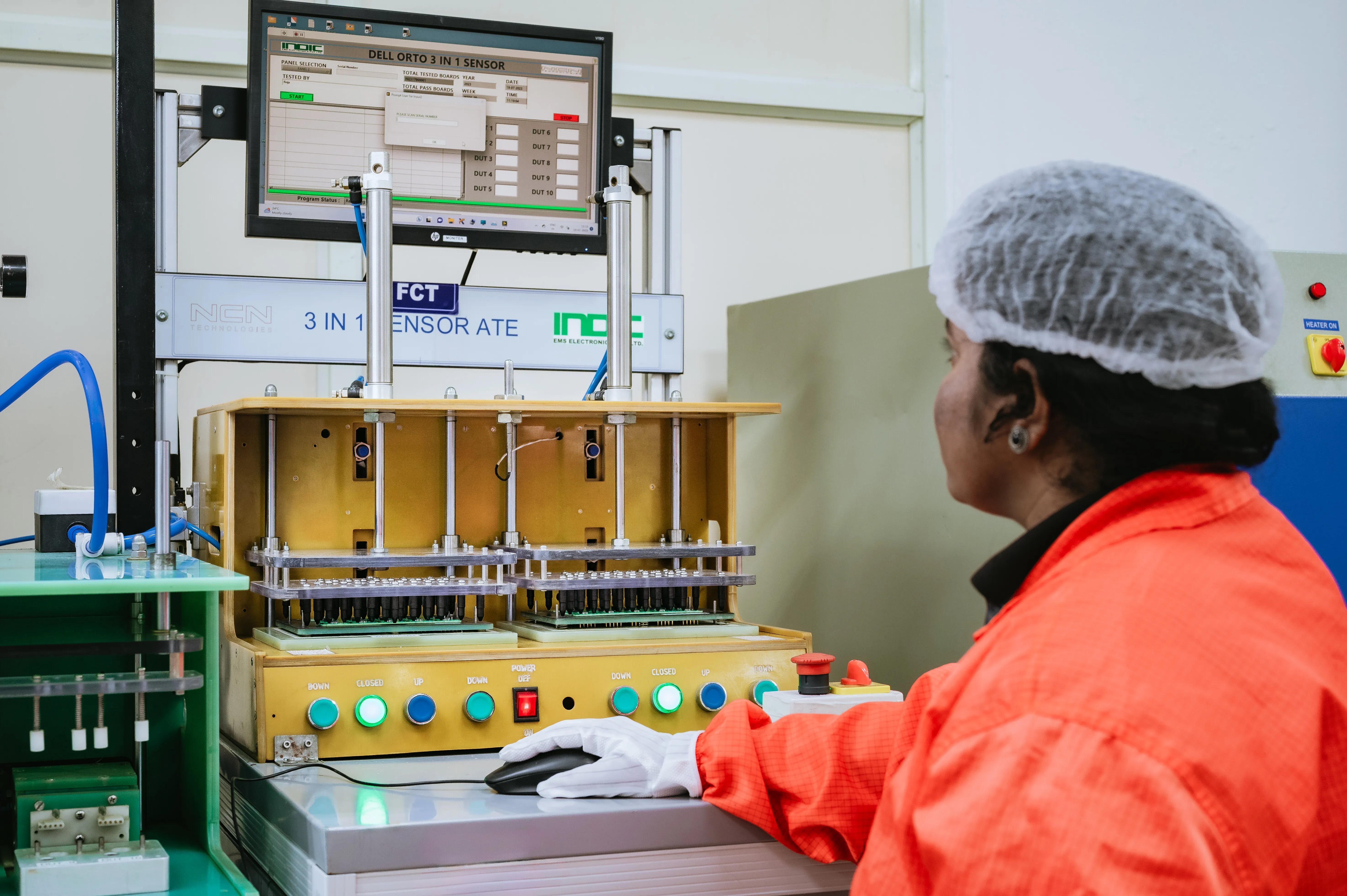
機能テスト
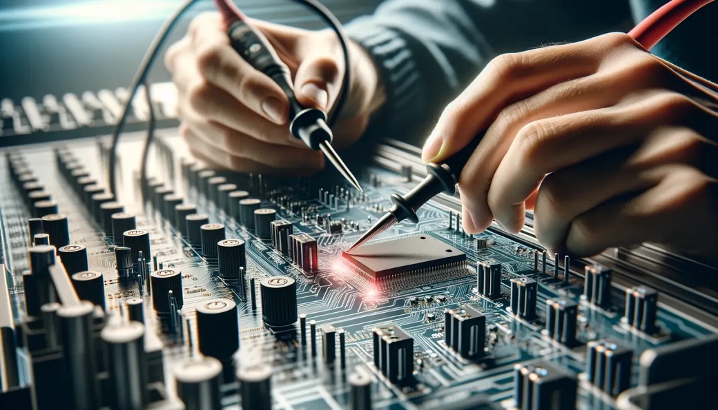
プリント回路基板アセンブリ(PCBA)の機能テスターは、組み立て後の電子回路の機能と性能を検証するために設計されたテストシステムです。機能テストは通常、PCBA が要求仕様を満たし、意図したとおりに動作することを確認するために、はんだ付けと組み立てのプロセスの後に実施されます。PCBA用ファンクションテスターのコンポーネントと機能の概要は次のとおりです。
テスト設定の概要
- テストフィクスチャ:
- テスト中にPCBを安全に配置するためのカスタム設計の固定具。
- PCBのフォームファクターとレイアウトに沿った精度と再現性を保証します。
- テストソフトウェア:
- 機能テスターの操作を制御し、カスタマイズされたテストルーチンを実行します。
- 特定の PCBA 要件に対応する定義済みのシーケンス、アルゴリズム、スクリプトが含まれています。
- データロギング、結果分析、およびレポート機能を提供します。
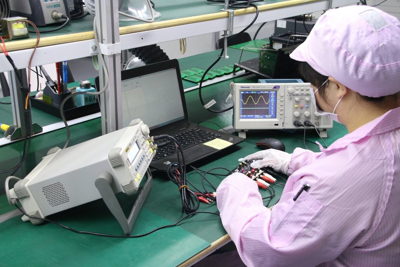
- インストルメンテーション:
- DMM、オシロスコープ、電源などのさまざまな機器を備えた機能テスター。
- 電圧、電流、波形、周波数を測定してPCBA機能を検証します。
- インターフェースハードウェア:
- テストフィクスチャー、機器、PCBA間の電気接続を提供します。
- コネクタ、ケーブル、リレー、スイッチ、シグナルコンディショニング回路が含まれます。
- ユーザーインターフェース:
- テストの設定、進行状況の監視、結果の表示を行うためのグラフィカルまたはテキストベースのインターフェイス。
- テスト選択メニュー、パラメータ設定、ステータスインジケータ、および結果表示を備えています。
- 機能テストの対象範囲:
- POST、信号処理、通信インターフェース、センサーキャリブレーションなど、さまざまな機能テストを実行します。
- スケーラビリティと柔軟性:
- PCB設計、テストニーズ、および生産量の変化に適応できます。
- モジュラーアーキテクチャと構成可能なセットアップにより、進化するテスト要件と複数の製品バリエーションを1つのプラットフォームでサポートします。
機能テストに対する当社のアプローチは、精度と効率性に根ざしています。自動テストと手動テスト方法を組み合わせて、電子機器のあらゆる側面を綿密に評価します。当社の経験豊富な技術者チームは、高度な試験装置を活用し、業界のベストプラクティスに従って実際のシナリオをシミュレートし、潜在的な問題を特定します。
私たちはあらゆる手段を講じています。当社の試験手順は、お客様の電子機器が最高水準の品質と信頼性を満たすよう、幅広い機能を網羅しています。インディック電子は最先端の試験設備と高度なツールを備えています。技術の進歩に遅れずについていくという当社の取り組みにより、最新の業界標準に沿った試験サービスを確実に提供しています。
Functional Testing for PCBA - Capabilities
- 当社の有資格テストエンジニアチームは、テストプリント回路基板とアセンブリを継続的に評価および開発しています。
- 機能テストには、I/O PCB、通信ポート、デジタルマルチメータなどの機器が必要です。
- 通常、テストはテストエンジニアが指示したテスト手順と仕様に従って行われます。
- テスターをプローブポイントを介してPCBに接続すると、PCBの電気環境を刺激します。
- したがって、テストが完全な証拠となり、設計または機能上の欠陥が明らかになるため、後日コストのかかる間違いが発生することがなくなります。


Functional Testing for PCBA - FAQ
Functional testing can identify a wide range of defects, including: Incorrect component installation (wrong orientation or placement). Faulty components (damaged or non-operational parts). Soldering issues (cold joints, solder bridges). Missing components or incorrect component values. Short circuits or open circuits within the PCB.
Functional testing in the Electronics Manufacturing Services (EMS) industry involves verifying that a completed electronic assembly, such as a PCB, operates according to its design specifications. This test checks the functionality of the device under test (DUT) by simulating its operational environment.
If a PCB fails functional testing: The failure is analyzed to determine the cause (component, assembly process, design issue). The PCB may undergo rework or repair to correct the identified issue. After repairs, the PCB is retested to ensure it now passes functional testing, verifying its readiness for final assembly.
PCB functional testing services are offered by EMS providers to test assembled PCBs for proper functionality. These services use specialized equipment and test setups to simulate operational conditions and verify product performance against specified criteria.
Functional testing is conducted by applying specific inputs to the PCB and measuring the outputs to compare against expected results. Test equipment may include signal generators, power supplies, and measurement devices, configured according to the PCB's operational specifications.
Functional testing is crucial in PCB assembly because it: Ensures the assembled PCB meets the design requirements. Identifies manufacturing defects or component failures. Guarantees product reliability and quality before market release.
PCB functional testing is a process where a printed circuit board (PCB) assembly is tested for its intended operation. It ensures that all components and circuits on the PCB work correctly together as designed.